
Planarization
Chemical-mechanical planarization (CMP) relies on surfactants to create an optimally mixed slurry with effective wetting properties. KRÜSS tensiometers measure surface tension to ensure slurry consistency, while foam analyzers assess and control undesirable foaming, crucial for maintaining process stability.

Wafer cleanliness
Ensuring contaminant-free wafer surfaces is fundamental for subsequent processing steps. Contact angle measurements are highly sensitive to contamination or cleaner residues, making them ideal for optimizing and quality-controlling various frontend cleaning steps. Our contact angle instruments provide precise assessments without compromising wafer integrity.
Contact us
Automated batch testing
For series QC checks for cleanliness or wettability, mobile contact angle instruments are combined with robotic systems, the software seamlessly communicates with surrounding systems via APIs or the OPC UA protocol to integrate the contact angle measurement step into the ensemble of test steps.
Experience how automated batch testing with our mobile instruments works in a customer story of the Fraunhofer CSP institute.
Go to customer story
Wire Bonding
For robust electrical connections during wire bonding, bond pads must be free from contamination and oxidation. Micro-scale contact angle measurements offer critical insights into surface conditions. Specialized micro equipment enables accurate evaluations using picoliter droplets, ensuring optimal surface preparation for reliable wire bonds.
More information
Glob top encapsulation
Protecting sensitive components through glob top encapsulation requires coatings with strong adhesion and appropriate interfacial tension. Our Drop Shape Analyzers facilitate the assessment of these parameters, contributing to the long-term stability and reliability of encapsulated semiconductor devices.
Contact us
Die underfilling
Effective underfilling with epoxy resin is vital to protect chips from mechanical stress and environmental factors. Optimal wetting ensures complete coverage and prevents air pockets. Our Drop Shape Analyzers support packaging engineers in evaluating wettability and calculating spreading speeds, facilitating efficient underfilling processes.
Contact us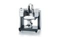
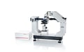
DSA100W
Automatic wettability and adhesion analysis of wafers and other round samples
Tensíío
The new generation tensiometer for liquid and solid surfaces
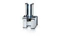
DFA100
The universal instrument for all aspects of liquid foam
Ayríís
Surface quality control has never been so easy and reliable

MSA One-Click SFE
Analyzing wettability in a second with only one click
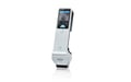
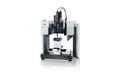
DSA30M
Precision wettability analysis of microscopically small surfaces
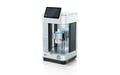
DSA100E
The automated premium solution for wetting and adhesion analysis of solids and liquids